
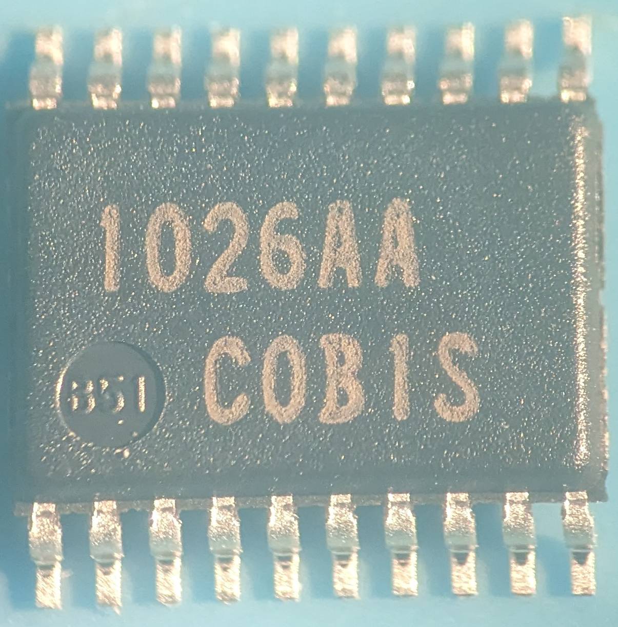
On October 22, 2026, Renesas announced the RX74M and RX74N, the new flagships of its 32-bit RX microcontroller family. According to the Renesas press release, they are the first RX parts built on a 22nm process and the first to use embedded MRAM in place of flash. Renesas says they run an RXv3e core at "up to 600 MHz" and deliver more than twice the performance of the 240 MHz RX72M and RX72N they sit above.
These are industrial parts. The RX74M targets AC drives, industrial robots and PLCs, and the RX74N targets smart meters, power conditioners and HVAC. They still matter to anyone writing firmware for a living, for three reasons: the memory technology changes how non-volatile writes work, the RX74M evaluation kit already has a board page in the Zephyr RTOS, and that kit carries the same expansion headers found on most hobbyist bench boards.
The core and the memory map
The RX74M product page lists a 600MHz RXv3e core rated at 6.01 CoreMark/MHz (typical) with a double-precision FPU. The page's parameter table also lists 300 and 480 MHz maximum-frequency options. Highways Today also reports 300, 480 and 600 MHz configurations. The press release says the 300 MHz products use more than 20% less power; CircuitDigest repeats that figure. Neither Renesas product page gives a power figure.
Renesas' product pages give the on-chip memory as:
- 1MB of code MRAM with dual bank (the parameter table also lists 512 KB program-memory variants)
- 48KB of data MRAM
- 1.5MB of SRAM with ECC (1536 KB in the parameter table)
The press release adds 256 KB of zero-wait-state TCM (tightly coupled memory). For code too large for the internal array, the RX74M page lists execute-in-place (XiP) from external octal flash or RAM with on-the-fly decryption.
The electrical and package specs are the same on both product pages: 1.62V to 3.63V supply, junction temperature from -40C to 125C, 100/144/176-pin QFP and 176/224/320-pin BGA packages, and "up to 197 I/O ports". One discrepancy: the RX74M parameter table lists I/O counts of 75, 103, 123, 162 and 200 across variants, so its top figure is higher than the 197 in the features list. The press release and CircuitDigest give the supply range as 1.62 V to 3.6 V. We use the 3.63V figure from the product pages.
Why MRAM instead of flash
The press release and CircuitDigest both make the same point. MRAM can be rewritten without first erasing it. NOR flash has to erase a whole block before reprogramming any part of it. That erase cycle is why flash-based firmware needs sector-sized buffers, wear-levelling layers for config storage, and careful scheduling around the stalls a flash erase causes.
With write-without-erase memory, logging calibration data, storing configuration or committing state just before power loss gets simpler. The 48KB data MRAM is a separate region from the code MRAM, which suits that kind of non-volatile data. The dual-bank code MRAM fits the usual pattern of writing a new image to one bank while running from the other. Renesas does not give MRAM endurance or retention figures on the pages we read, so we have none to report.
RX74M vs RX74N: where they differ
The connectivity list separates the two parts. On the RX74M page, Renesas lists:
- a built-in EtherCAT slave controller
- 2ch Gigabit EtherMAC
- an L3 Ethernet switch with TSN
- USB 2.0 Host/Function/OTG
- CAN FD (ISO 11898-1-2015, up to 150Mbps)
- an SD host
The press release says the RX74M supports EtherCAT, PROFINET and EtherNet/IP, including DLR (Device Level Ring).
The RX74N page describes that part as a "High-Performance Flagship MCU with Integrated Gigabit Ethernet Connectivity for Industrial Applications". It lists the same core, memory, voltage range and packages, plus USB 2.0 Host/Function/OTG, CAN FD, a 16-bit A/D and a 12-bit D/A. It does not list the built-in EtherCAT controller that the RX74M page does. In short, the RX74M is the industrial-fieldbus part and the RX74N is the Ethernet-connected control part for energy and building systems.
For security, the RX74N page lists crypto engines for AES, ChaCha20, RSA, ECC, SHA512 and SHA3-512, plus tamper detection and ProtectZone. The press release describes ProtectZone as a feature of the RX CPU and pairs it with next-generation Renesas Secure IP (RSIP) with authenticated encryption. Renesas presents the security features in terms of compliance with the EU Cyber Resilience Act (CRA) and post-quantum cryptography. The press release also quotes Yoshi Ishikawa, Senior Director of the EP Advanced MCU Business Division at Renesas.
The EK-RX74M and Zephyr
The Zephyr Project documentation already has a page for the RX74M Evaluation Kit. It lists board ek_rx74m, SoC r5k574mcb4ae, architecture rx and status "Maintained". According to that page, the kit has:
- the 600 MHz RX74M (R5K574MCB4AE) in a 320-pin LFBGA
- 512 Mbit of external OctaFlash and 256 Mbit of external OctalRAM
- a 24.000 MHz main crystal and a 32.768 kHz sub crystal
- an on-board E2 emulator for debugging
- an Arduino Uno R3 connector, a mikroBUS socket and two Digilent Pmod connectors
- Grove and Qwiic footprints, which ship unpopulated
- CAN FD, the L3 Ethernet switch/EtherCAT slave controller with 2 Ethernet ports, and USB HS/FS
A Zephyr board page in launch week means engineers can try the part without committing to a vendor-only toolchain. The Arduino, mikroBUS and Pmod headers mean existing shields and click boards can be wired up without a custom adapter. The Zephyr page does not say which drivers are supported at this point, and we did not verify which peripherals have upstream drivers.
What It Means for Makers
These chips are aimed at drive, robot, PLC and grid-equipment designers. Hobbyists are unlikely to put a 320-pin BGA on a home-made board. The people who will find the RX74M and RX74N useful are embedded engineers and advanced makers working on motor control, industrial networking, or Ethernet-connected data logging and control. For RX users, the parts are the upgrade path above the 240 MHz RX72M and RX72N. For newcomers, the EK-RX74M is the easy entry point because of its on-board debugger, its standard expansion headers and its Zephyr board support.
What the parts make possible: an EtherCAT or PROFINET node with TSN switching and CAN FD on one chip (RX74M), and firmware storage that writes without erasing. The second is the more interesting change for anyone who has had to work around flash erase limits for data logging.
Status and pricing: the press release says the RX74M and RX74N are "available today", and both product pages are marked "NEW" and "Active" with an "Order Now" button. We found no unit pricing, no EK-RX74M kit price and no volume-availability date on any page we read. We will update this story when Renesas publishes figures.
Sources
- Renesas Launches RX74M and RX74N Flagship 32-bit MCUs, First RX Family Built on 22nm Process and Featuring MRAM (Renesas, Oct 22, 2026)
- RX74M product page (Renesas)
- RX74N product page (Renesas)
- RX74M Evaluation Kit (EK-RX74M), Zephyr Project documentation
- Renesas Takes Its RX MCUs to 600 MHz and Swaps Flash for MRAM With the New 22nm RX74M and RX74N (CircuitDigest, Oct 23, 2026)
- Renesas Brings 600 MHz Processing and MRAM to Industrial Automation (Highways Today, Oct 23, 2026)
