
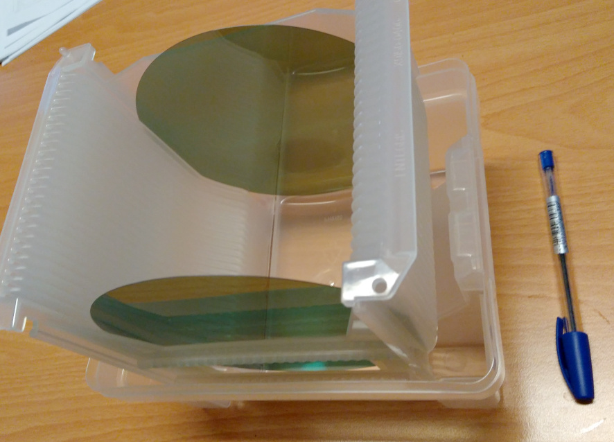
Infineon Technologies says it has processed 300 mm silicon-carbide (SiC) wafers into functional power devices, and is calling it a world first. The announcement came from Munich on 9 November 2026. The work was done at the company's fab in Villach, Austria, and according to Infineon it ran on existing silicon manufacturing equipment rather than a dedicated SiC line. The company is showing the result at electronica in Munich, Hall C3, Booth 502, from 10 to 13 November.
Read the announcement carefully. Infineon is not saying 300 mm SiC parts are in production, sampling or on sale. It says it has made working devices on the larger wafer format and will now plan the technology and the ramp timing together with customers and partners. No date is attached. Hackster.io's independent coverage calls it "an early success" and notes that ramp planning is still under way with customers and partners.
What Infineon Actually Claims
Taken together, Infineon's press release and the trade-press reports describe four specific claims:
- Functional devices on 300 mm SiC. SiC wafers of 300 mm diameter were processed into power devices that work, at Villach. Neither the press release nor the coverage we checked names the device types, voltage classes or yield figures, so we won't guess at them.
- Existing silicon equipment. Infineon says the processing used tools already in place for silicon manufacturing. Electronics Weekly reports the same detail. This is the most interesting part of the announcement from a manufacturing point of view. Sharing tools with a silicon line, if it holds up at volume, avoids building a separate fleet of equipment for SiC.
- 2.3 times more chips per wafer. According to Infineon, a 300 mm wafer gives 2.3 times as many chips as a 200 mm wafer. This is the company's own figure. It is not a measured yield from production.
- Cold Split on 300 mm. Separately, Infineon says it has proven Cold Split feasibility on 300 mm SiC at its Dresden site. Cold Split is a wafer-separation process. Infineon says it causes less material loss and takes less processing time than conventional wire sawing.
Infineon also says it will keep executing its 200 mm SiC manufacturing roadmap in parallel. So 300 mm adds to the current plan; it does not replace it, at least for now.
Why Wafer Diameter Matters
Power semiconductors are priced largely on how many good dies come off each wafer, and on what it costs to process that wafer. A bigger wafer spreads many of the fixed processing steps across more chips. The 2.3x figure is Infineon's way of putting that advantage in numbers. Doing it on equipment the company already owns is the second half of the cost argument.
The announcement also fits a pattern in Infineon's recent messaging. Hackster.io notes that the company can now produce on 300 mm wafers in silicon, gallium nitride (GaN) and now SiC. On 27 October 2026, Infineon announced an investment of approximately EUR 1.1 billion in a high-volume manufacturing facility for GaN power semiconductors on 300 mm wafers, also in Villach. Infineon's press release presents the SiC result as extending that approach to a second wide-bandgap material.
CEO Jochen Hanebeck is quoted in the press release presenting the result as a technological milestone. The quote does not add specs, prices or dates.
Where These Devices End Up
Electronics Weekly lists the applications where SiC power devices are used: traction inverters, on-board chargers, EV chargers, large-scale energy storage, industrial drives and uninterruptible power supplies (UPS), with rising demand in AI data centres. These are high-power, high-voltage systems. None of them is a hobbyist bench project, and the announcement makes no claim about low-power or maker-class parts.
What It Means for Makers
Who it is for: automotive, industrial and energy-infrastructure customers that design power conversion stages with SiC power devices, together with the fabs and supply-chain planners who serve them. Infineon says ramp timing will be worked out with its customers and partners.
What it replaces or enables: nothing you can buy today. If the format reaches volume, a 300 mm process would sit next to Infineon's 200 mm SiC production rather than replace it, since the company says the 200 mm roadmap continues. The most a maker or small-shop engineer can reasonably expect is an indirect effect further down the line: more SiC dies per wafer is the kind of change that can eventually show up in supply and pricing for SiC parts at the distributor level. None of the sources makes that pricing claim, and we are not making it either.
Price and availability: none. The sources give no price, no part numbers, no sampling programme and no ramp date. The status is a manufacturing milestone, announced on 9 November 2026. It is not pre-order, not sampling and not shipping. If you are at electronica this week, the demonstration is at Hall C3, Booth 502, from 10 to 13 November.
For anyone following power-electronics supply, the details to watch for in later Infineon disclosures are concrete ones: which device families come first on 300 mm, the voltage classes, whether yields on shared silicon tools match those of dedicated SiC lines, and when the ramp schedule agreed with customers becomes public. Until then, treat this as a credible early engineering result with the commercial timeline still open.
